
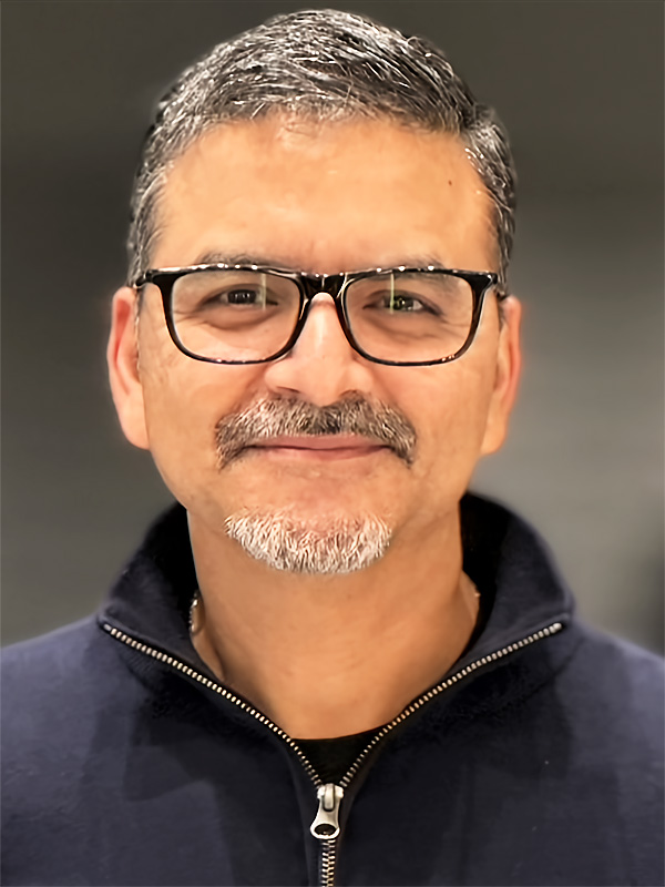
Sandeep Kumar Goel
Senior Director
Taiwan Semiconductor Manufacturing Company (TSMC),
San Jose, CA
The convergence of aggressive process scaling at leading-edge nodes and the adoption of 3D IC architectures presents unprecedented challenges for semiconductor test. From a foundry perspective, addressing these challenges is critical to accelerating yield learning, reducing test cost, and ensuring high reliability. This keynote explores the evolving test landscape across both advanced nodes and 3D integration. We will first discuss the testing complexities that arise when migrating to advanced nodes, highlighting the difficulties in detecting and screening subtle marginal defects caused by severe process variations, as well as the mounting hurdles in physical defect diagnosis. In addition, we will examine strategies to make testing more effective at targeting and mitigating systematic defects driven by complex design-process interactions. The talk will then shift to 3D IC testing challenges, covering Known Good Die (KGD) test strategies, high-density vertical interconnect test, and the validation of stacked die configurations. Furthermore, we will explore how these test challenges evolve with the integration of silicon photonics, particularly regarding electro-optical co-testing, optical coupling, and thermal sensitivity. Finally, we will outline future directions in test methodologies, fault isolation, and optimized test flows from wafer-level to final stack test, providing a clear path forward for next-generation semiconductor manufacturing.
Sandeep Kumar Goel is an academician and Senior Director with Taiwan Semiconductor Manufacturing Company (TSMC), San Jose, CA. He received his M.Tech. degree in VLSI from IIT Delhi in 1999 and his Ph.D. in electrical and computer engineering from the University of Twente in 2005. He has co-authored two books, three book chapters, and published over 100 papers in journals and conference/workshop proceedings. Dr. Goel holds more than 100 granted U.S. patents and has several others pending.
He was the recipient of the Most Significant Paper Award at the IEEE International Test Conference in 2010, the IEEE Computer Society Distinguished Contributor Award in 2022, and the IEEE SA Emerging Technology Award in 2026 for IEEE Std. P3537. He has delivered keynotes and invited talks at several premier conferences, including DAC, ICCAD, ETS, and 3DIC. He served as the General Chair of the 3D Workshop at DATE 2012, the Vice-Program Chair for ITC 2025, the Program Chair for ITC 2026, and is the General Chair for ITC 2027. Dr. Goel is a Fellow of the IEEE and chairs the IEEE Std. P3537 Standard for 3Dblox: Chiplet connectivity and physical properties description language.
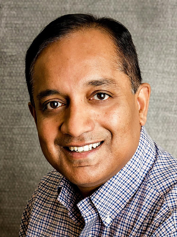
Nilanjan Mukherjee
VP of Software Engineering
Siemens EDA
The semiconductor industry's progression toward advanced technology nodes, elevated transistor densities, and heterogeneous integration within complex packages has intensified the challenges associated with ensuring high quality and reliability of integrated circuits. This evolution coincides with exponential growth in infrastructure requirements spanning data generation, transmission, storage, analysis, and monetization. Modern computing paradigms, particularly continuous AI/ML training and inference workloads, impose unprecedented operational demands on semiconductor ICs, fundamentally altering traditional reliability assumptions.
The conventional paradigm of manufacturing-phase testing followed by field deployment under the assumption of sustained operational integrity is no longer adequate. Continuous in-situ monitoring has emerged as a critical necessity for maintaining device reliability throughout the operational lifecycle.
This presentation examines three interconnected aspects of modern semiconductor test and reliability: (1) the evolving test quality challenges confronting the industry in advanced technology nodes, (2) the sophisticated Design-for-Test (DFT) infrastructure architectures developed to enhance test coverage and effectiveness across the entire product lifecycle, and (3) the strategic deployment of integrated monitors and sensors to enable predictive maintenance methodologies, thereby enhancing overall device reliability and operational longevity.
Nilanjan Mukherjee is Vice President of Software Engineering for Tessent Silicon Lifecycle Solutions at Siemens EDA, where he leads the development of transformative technologies that span the complete lifecycle of silicon—from design through field operation.
Throughout his career, Nilanjan has been instrumental in advancing critical areas of semiconductor testing and diagnostics, including test quality, test compression, Logic BIST, Memory BIST, low-power DFT, and failure diagnosis. His technical contributions include pioneering work on EDT/TestKompress, VersaPoint Test Points technology, Low-power hybrid EDT/Logic BIST scheme, Observation Scan Technology, and In-Field Testing using packetized scan data through SSN. More recently, he has championed the industry shift toward early DFT validation through RTL-level analysis and insertion tools that enable "Shift-Left DFT" methodologies.
His current focus centers on silicon lifecycle management—integrating on-chip sensors and monitors during test phases and leveraging data analytics to correlate failures across functional and structural operating modes, enabling predictive and proactive silicon health management.
Nilanjan's contributions have earned significant recognition: he holds 60+ US patents and numerous international patents and has co-authored over 100 peer-reviewed technical papers. His work has been honored with Best Paper Awards at VTS (2020), VLSI Design (2009), ATS (2001), and VTS (1995); the Most Significant Paper Award at ITC (2012); the Siemens DISW Invention of the Year (2019); and the IEEE Donald O. Pederson Outstanding Paper Award (2006).
Nilanjan is a sought-after speaker and educator, having delivered tutorials and invited talks at premier conferences including DAC, ITC, VTS, ATS, and VLSI Design, and has developed and taught numerous short-term courses on DFT methodologies.

Michael Campbell
Senior Vice President of Engineering for QUALCOMM CDMA Technologies
Artificial intelligence is transforming the semiconductor industry at unprecedented speed. AI-driven devices are increasing in scale, power, integration, and complexity, creating new challenges across design, manufacturing, test, yield, and reliability. Traditional semiconductor test methodologies, which have evolved successfully for decades, are reaching their limits as complexity and thermal loads move into the kilowatt range, heterogeneous and 3D integration reduce physical observability, test insertions multiply, and the volume of engineering data grows dramatically.
This presentation explores how AI can become part of the solution to the complexity it helped create. The presentation discusses the growth of Fabs and SATs that are a result of the explosive growth of AI’s use of semiconductors. Due to all the changes in flux, the next generation of semiconductor test will require testability, and observability of system failures to move earlier into architecture and design, with tighter connections between pre-silicon and post-silicon engineering. Equally important, fragmented data must evolve into a governed, connected, AI-ready foundation that enables information and learning to flow across design, DFT, wafer test, ATE, system-level test, diagnostics, failure analysis, and manufacturing.
The result is a transition from isolated automation toward an intelligent semiconductor ecosystem in which AI agents help engineers generate test content, analyze increasingly complex data, execute characterization, diagnose failures, optimize test strategies, and continuously learn across products and test insertions. Human engineering judgment remains at the center, but engineers increasingly work alongside a coordinated “AI team” capable of operating continuously and at a scale that traditional tools cannot achieve.
The fundamental shift is not simply using AI to make today’s test processes faster. It is using AI, connected data, and human expertise to reinvent how semiconductor test learns, adapts, and operates in the age of intelligent silicon.
Michael Campbell is Senior Vice President of Engineering for QUALCOMM CDMA Technologies, (QCT), where he leads Product and Test Engineering, Test Automation, Failure Analysis, and Yield.
Michael joined Qualcomm in 1996. At Qualcomm, Michael has led teams across multiple areas of the business including Design Automation, FA, Yield Optimization, Product Development & Test Engineering (PDTE), Foundry Semiconductor Analysis, and Quality. Since 2014 he has been driving ML & AI test optimization internally & externally with key ATE/EDA providers for value-add AI in the test world. His drive has enabled AI boxes at multiple tester companies that enable in line real time AI functions to drive and deliver improvements in test quality and cost.
During his career at Qualcomm, Michael also has brought up Design and Test facilities in Bangalore, Singapore, Taiwan, and Mexico. In his current role, he is working to change the business and supply change through changes in PDTE and FA by driving machine learning using data available from semiconductor test to train models and automate processes.
Prior to joining QUALCOMM, Michael held engineering roles at several companies, including Mostek, INMOS and Honeywell. He holds a Bachelor of Science degree in Electrical Engineering and Computer Engineering from Clarkson University.

Adam Cron
Distinguished Architect
Synopsys
The Heterogeneous Integration Roadmap is getting an update as you read this. Keeping up with Moore’s Law has driven electronics manufacturing to multi-die packaging options that pack more transistors into a unit of area than ever before. This has strained the limits of power delivery networks, thermal mitigation techniques, test data volumes and their data delivery mechanisms. This talk will discuss these areas and the pressures focused on threading the needle between test and profitability, reviewing key industry challenges and technology directions enabling scalable logic test in future semiconductor systems.
Adam Cron is a Distinguished Architect at Synopsys working with customers worldwide on complex Test, Security, and Silicon Lifecycle Management tool flows and architectures for digital ICs. He has helped architect design-for-test, design-for-manufacturing, and security tools for several generations of products. As a Syracuse University Computer Engineering graduate, Adam also worked in test-related fields at Motorola and Texas Instruments where he got his first exposure to IEEE standards while designing the first ICs compliant to IEEE Std 1149.1. In the past, Adam had served as Chair or Vice-chair of the Test Technology Standards Committee overseeing the development of IEEE Test Standards for about a dozen years. Adam is Chair of IEEE Std 1838 which standardized 3D-IC test access; Editor of IEEE Std 1149.4 for a mixed-signal test bus; a member on many IEEE Test Standards working groups such as P1687, P1687.2, P2929, etc.; an IEEE Golden Core recipient, recipient of the 2024 IEEE Computer Society Hans Karlsson Standards Award, and a 2025 recipient of the IEEE SA Lifetime Achievement Award “for continuous and outstanding service to the standards development community in the field of electronic testing and design-for-test solutions.” He has authored several papers, articles, book chapters, and patents and is a frequent speaker or panelist at conference sessions held at events such as ITC and DAC.
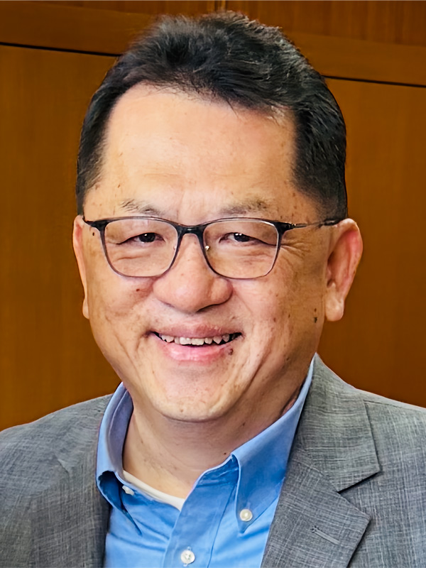
Clark Liu
Chief Technology Marketing Officer, MJC
Taiwan Program Chair, SWTEST
Asia
SEMI Taiwan, Testing Committee
Vice President, HiSPA
Traditional semiconductor test focuses on electrical signal integrity and scalable probe card flows. In contrast, SiPh/CPO testing introduces hybrid optical-electrical domains requiring sub-micron optical alignment, high-speed electro-optical wafer probing, and fiber-attached module validation. System-level testing under multi-kilowatt thermal loads further raises complexity. This keynote outlines the four critical multi-stage insertions (1–4) and highlights how testing paradigms must evolve to ensure yield and reliability in next-generation heterogeneous integration.